- 您现在的位置:买卖IC网 > Sheet目录1999 > ICS9EX21831AKLF (IDT, Integrated Device Technology Inc)IC FANOUT/BUFFER DIFF 72VFQFN
IDT
Eighteen Output Differential Buffer w/2 input mux for PCIe Gen1/2/3
1678D—03/23/12
9EX21831
Eighteen Output Differential Buffer w/2 input mux for PCIe Gen1/2/3
4
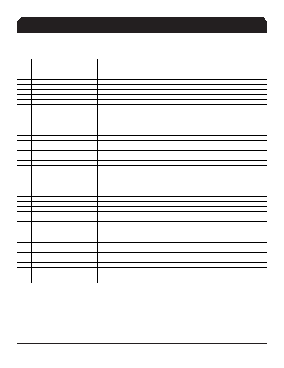
Pin Description (Continued)
37
DIF_0
OUT
0.7V differential true clock output
38
DIF_0#
OUT
0.7V differential complement clock output
39
DIF_1
OUT
0.7V differential true clock output
40
DIF_1#
OUT
0.7V differential complement clock output
41
DIF_2
OUT
0.7V differential true clock output
42
DIF_2#
OUT
0.7V differential complement clock output
43
VDD
PWR
Power supply, nominal 3.3V
44
GND
PWR
Ground pin.
45
DIF_3
OUT
0.7V differential true clock output
46
DIF_3#
OUT
0.7V differential complement clock output
47
DIF_4
OUT
0.7V differential true clock output
48
DIF_4#
OUT
0.7V differential complement clock output
49
OE5#
IN
Active low input for enabling DIF pair 5.
1 = tri-state outputs, 0 = enable outputs
50
DIF_5
OUT
0.7V differential true clock output
51
DIF_5#
OUT
0.7V differential complement clock output
52
OE6#
IN
Active low input for enabling DIF pair 6.
1 = tri-state outputs, 0 = enable outputs
53
DIF_6
OUT
0.7V differential true clock output
54
DIF_6#
OUT
0.7V differential complement clock output
55
VDD
PWR
Power supply, nominal 3.3V
56
OE7#
IN
Active low input for enabling DIF pair 7.
1 = tri-state outputs, 0 = enable outputs
57
DIF_7
OUT
0.7V differential true clock output
58
DIF_7#
OUT
0.7V differential complement clock output
59
OE8#
IN
Active low input for enabling DIF pair 8.
1 = tri-state outputs, 0 = enable outputs
60
DIF_8
OUT
0.7V differential true clock output
61
DIF_8#
OUT
0.7V differential complement clock output
62
VDD
PWR
Power supply, nominal 3.3V
63
HIBW_BYPM_LOBW#
IN
Trilevel input to select High BW, Bypass Mode or Low BW.
0 = Low BW Mode, Mid= Bypass Mode, 1 = High Bandwidth
64
SMBCLK
IN
Clock pin of SMBUS circuitry, 5V tolerant
65
SMBDAT
I/O
Data pin of SMBUS circuitry, 5V tolerant
66
SMB_A1
IN
SMBus address bit 1
67
SMB_A0
IN
SMBus address bit 0 (LSB)
68
SEL_A_B#
IN
Input to select differential input clock A or differential input clock B.
0 = Input B selected, 1 = Input A selected.
69
CKPWRGD/PD#
IN
Notifies the clock to sample latched inputs on the rising edge, and to power down on the falling
edge.
70
DIF_9
OUT
0.7V differential true clock output
71
DIF_9#
OUT
0.7V differential complement clock output
72
OE9#
IN
Active low input for enabling DIF pair 9.
1 = tri-state outputs, 0 = enable outputs
发布紧急采购,3分钟左右您将得到回复。
相关PDF资料
ICS9FG1901HKLFT
IC FREQUENCY GENERATOR 72-QFN
ID82C54
IC OSC PROG TIMER 8MHZ 24DIP
IDT2308A-4DCI8
IC CLOCK MULT ZD HI DRV 16-SOIC
IDT2309-1HPGGI
IC CLK BUFFER ZD HI DRV 16-TSSOP
IDT2309A-1HPGG
IC CLK BUFFER ZD HI DRV 16-TSSOP
IDT2309B-1HPGGI
IC CLK BUFFER HIGH DRIVE 16TSSOP
IDT23S05-1HDCGI
IC CLK BUFFER PLL HI DRV 8-SOIC
IDT23S05E-1HDCGI8
IC CLK BUFFER PLL HI DRV 8-SOIC
相关代理商/技术参数
ICS9EX21831AKLFT
功能描述:IC FANOUT/BUFFER DIFF 72VFQFN RoHS:是 类别:集成电路 (IC) >> 时钟/计时 - 专用 系列:PCI Express® (PCIe) 标准包装:1,500 系列:- 类型:时钟缓冲器/驱动器 PLL:是 主要目的:- 输入:- 输出:- 电路数:- 比率 - 输入:输出:- 差分 - 输入:输出:- 频率 - 最大:- 电源电压:3.3V 工作温度:0°C ~ 70°C 安装类型:表面贴装 封装/外壳:28-SSOP(0.209",5.30mm 宽) 供应商设备封装:28-SSOP 包装:带卷 (TR) 其它名称:93786AFT
ICS9FG1001AGLF
功能描述:IC GENERATOR ZD FREQ 56-TSSOP RoHS:是 类别:集成电路 (IC) >> 时钟/计时 - 专用 系列:PCI Express® (PCIe) 标准包装:1,500 系列:- 类型:时钟缓冲器/驱动器 PLL:是 主要目的:- 输入:- 输出:- 电路数:- 比率 - 输入:输出:- 差分 - 输入:输出:- 频率 - 最大:- 电源电压:3.3V 工作温度:0°C ~ 70°C 安装类型:表面贴装 封装/外壳:28-SSOP(0.209",5.30mm 宽) 供应商设备封装:28-SSOP 包装:带卷 (TR) 其它名称:93786AFT
ICS9FG1001AGLFT
功能描述:IC GENERATOR ZD FREQ 56-TSSOP RoHS:是 类别:集成电路 (IC) >> 时钟/计时 - 专用 系列:PCI Express® (PCIe) 标准包装:1,500 系列:- 类型:时钟缓冲器/驱动器 PLL:是 主要目的:- 输入:- 输出:- 电路数:- 比率 - 输入:输出:- 差分 - 输入:输出:- 频率 - 最大:- 电源电压:3.3V 工作温度:0°C ~ 70°C 安装类型:表面贴装 封装/外壳:28-SSOP(0.209",5.30mm 宽) 供应商设备封装:28-SSOP 包装:带卷 (TR) 其它名称:93786AFT
ICS9FG1001BGLF
功能描述:IC GENERATOR ZD FREQ 56TSSOP RoHS:是 类别:集成电路 (IC) >> 时钟/计时 - 专用 系列:* 标准包装:28 系列:- 类型:时钟/频率发生器 PLL:是 主要目的:Intel CPU 服务器 输入:时钟 输出:LVCMOS 电路数:1 比率 - 输入:输出:3:22 差分 - 输入:输出:无/是 频率 - 最大:400MHz 电源电压:3.135 V ~ 3.465 V 工作温度:0°C ~ 85°C 安装类型:表面贴装 封装/外壳:64-TFSOP (0.240",6.10mm 宽) 供应商设备封装:64-TSSOP 包装:管件
ICS9FG1001BGLFT
功能描述:IC GENERATOR ZD FREQ 56TSSOP RoHS:是 类别:集成电路 (IC) >> 时钟/计时 - 专用 系列:* 标准包装:28 系列:- 类型:时钟/频率发生器 PLL:是 主要目的:Intel CPU 服务器 输入:时钟 输出:LVCMOS 电路数:1 比率 - 输入:输出:3:22 差分 - 输入:输出:无/是 频率 - 最大:400MHz 电源电压:3.135 V ~ 3.465 V 工作温度:0°C ~ 85°C 安装类型:表面贴装 封装/外壳:64-TFSOP (0.240",6.10mm 宽) 供应商设备封装:64-TSSOP 包装:管件
ICS9FG104CGLF
功能描述:IC FREQ TIMING GENERATOR 28TSSOP RoHS:是 类别:集成电路 (IC) >> 时钟/计时 - 专用 系列:PCI Express® (PCIe) 标准包装:1 系列:- 类型:时钟/频率发生器,多路复用器 PLL:是 主要目的:存储器,RDRAM 输入:晶体 输出:LVCMOS 电路数:1 比率 - 输入:输出:1:2 差分 - 输入:输出:无/是 频率 - 最大:400MHz 电源电压:3 V ~ 3.6 V 工作温度:0°C ~ 85°C 安装类型:表面贴装 封装/外壳:16-TSSOP(0.173",4.40mm 宽) 供应商设备封装:16-TSSOP 包装:Digi-Reel® 其它名称:296-6719-6
ICS9FG104CGLFT
功能描述:IC FREQ TIMING GENERATOR 28TSSOP RoHS:是 类别:集成电路 (IC) >> 时钟/计时 - 专用 系列:PCI Express® (PCIe) 标准包装:1 系列:- 类型:时钟/频率发生器,多路复用器 PLL:是 主要目的:存储器,RDRAM 输入:晶体 输出:LVCMOS 电路数:1 比率 - 输入:输出:1:2 差分 - 输入:输出:无/是 频率 - 最大:400MHz 电源电压:3 V ~ 3.6 V 工作温度:0°C ~ 85°C 安装类型:表面贴装 封装/外壳:16-TSSOP(0.173",4.40mm 宽) 供应商设备封装:16-TSSOP 包装:Digi-Reel® 其它名称:296-6719-6
ICS9FG104DFILF
功能描述:IC FREQ TIMING GENERATOR 28-SSOP RoHS:是 类别:集成电路 (IC) >> 时钟/计时 - 专用 系列:PCI Express® (PCIe) 标准包装:28 系列:- 类型:时钟/频率发生器 PLL:是 主要目的:Intel CPU 服务器 输入:时钟 输出:LVCMOS 电路数:1 比率 - 输入:输出:3:22 差分 - 输入:输出:无/是 频率 - 最大:400MHz 电源电压:3.135 V ~ 3.465 V 工作温度:0°C ~ 85°C 安装类型:表面贴装 封装/外壳:64-TFSOP (0.240",6.10mm 宽) 供应商设备封装:64-TSSOP 包装:管件